Memory Upgrade
(Most text and drawings provided by Leslie Ayling)
There are several ways to increase the memory of a System 80, each with their own pros and cons.
Piggyback Method
Get hold of 8 (for 32k) or 16 (for 48k)
4116 memory chips. Bend pin 15 horizontally on each of the chips and "piggyback"
them to the existing memory chips (soldering each of the legs very carefully).
Refer to the diagram below, and main CPU board schematics in the System
80 technical manual.
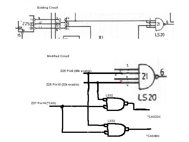
Z25 (Ls139) uses A14 and A15 to divide the the memory map into 4 areas,
providing active low enables for each. Normally only the the ROM (00)
and first 16k bank (01) enables are used.
Note: X2 will allow you to enable the ROMS in the C000-FFFF space for testing. Z21 is a 4 input NAND gate that uses these two outputs to enable the DATA BUS buffers. Z21 can easily be modified to enable the buffers in the 8000-FFFF range by making the changes as shown. The *CAS32 and *CAS48 signals are then run to pin 15 of the piggybacked RAM chips.
Alternative Method 1
This involves less soldering but is slightly more difficult. Nevertheless it is a much neater way of doing it, plus 4164 chips should be easier to get than 4116's these days. It also makes it easier to experiment with re-mapping the Address bus for CP/M since you have 64k of RAM available to play with. Here is the general approach...
Get 8 x 4164 Memory chips. They must be ones that have a 7x16 matrix as opposed to an 8x8 otherwise half the address space will not refresh due to the Z80 only providing a 7 bit refresh. I understand that some of the later Z80 variants (Z80H anyone confirm this?) provide an 8 bit refresh, so if you wanted to upgrade the processor this shouldn't be a problem. Replace the 4116's on the Motherboard with the 4164's. The +12v and -5v rails need to be disconnected from the RAM chips since the 4164's only need +5v and GND. A14 and A15 need to be multiplexed through the spare gate of Z24, and applied to the extra address pin of the 4164 chips. The data buffers need to be enabled for the 8000-FFFF space in the same way as for method 1 (above).
A step-by-step description of this method has been describe in a 2015 document written by a Matthew Bull, a System 80 enthusiast known on the New Zealand Vintage Computer Forums and the Vintage Computer Federation Forums as 3PCEDEV. This document can be downloaded here for those that might want to attempt this with a vintage System 80.
A company in New Zealand, John Gilbert & Company Ltd, produced similar instructions for the same 64k memory upgrade back in the day. However, these notes are sketchy and rough compared to Matthew's rewrite linked above. Nevertheless I've left the John Gilbert guide here purely for the historical record.
Alternative Method 2
Use 2 x 32k static RAM chips.
The CACHE ram chips found in most modern IBM compatibles should be suitable.
They have access times as low as 15ns (faster still?) and can be easily
battery backed. This will allow you to experiment with VERY fast Z80 chips
(assuming that you replace your system ROMs with a modern day FLASH ROM,
some of which have very low access times and come in DIP packages.)
This is the least trivial but the most flexible of the options. Since with some slight modifications to the System ROMS, and a faster processor you could have several "virtual System-80/Trs80's" running in their own address spaces a'la AMIGA. Each time the processor switches tasks/memory areas, it could just save the current screen contents/pointers into the relevant bank.